Verified MethodologyPrimary Evidence 45% · Comparative Specs 30% · Community Consensus 25%
NVIDIA Blackwell vs. Google TPU V6e? Top 10 AI Datacenter Chips & Accelerators in 2026
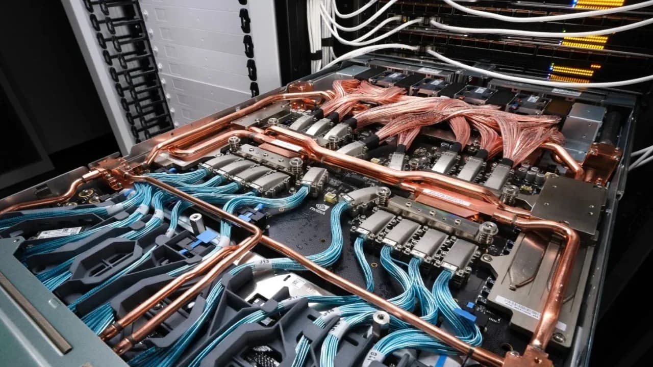
Frontier AI infrastructure in 2026 is no longer a one-architecture race. While NVIDIA's Blackwell B200 and GB200 NVL72 pack up to 288 GB of HBM3e memory and 1.8 TB/s NVLink 5 scale-up…
Read more
fabrics, hyperscalers and specialized silicon challengers are splitting prefill and decode apart with Google Cloud TPU v6e (Trillium), AMD Instinct MI355X, Microsoft Azure Maia 200, and Cerebras WSE-3. We ranked the top 10 AI datacenter chips and accelerators of 2026 across Compute & Memory Bandwidth (35%), Cluster Scale-Up Fabric (25%), Software Stack & Ecosystem Maturity (25%), and Price-Performance / Perf-per-Watt (15%).
tweaktown.com

Starting order. Vote up or down to reorder this list.
Current Rankings
- #1 Top RankedLeader
Fusing two TSMC 4NP reticle-limit dies across a 10 TB/s NV-HBI link into a single unified CUDA processor, NVIDIA Blackwell delivers 180 GB of HBM3e on B200 and up to 288 GB at 8 TB/s on Blackwell Ultra. In GB200 NVL72 liquid-cooled racks, 72 GPUs act as one giant 130 TB/s memory-coherent accelerator.
Key Benchmarks & Specifications
Memory & BW180–288 GB HBM3e8.0 TB/sPeak Compute9 PFLOPS FP815–18 PFLOPS FP4Scale-Up Fabric1.8 TB/s NVLink 5 (72-GPU Domain)Maker & Process NVIDIA (TSMC4NP)Editorial Strengths & Watchouts
+ Strengths / Pros
- +72-GPU NVLink 5 domain (1.8 TB/s per GPU) crushes multi-node MoE communication bottlenecks
- +Up to 288 GB HBM3e at 8 TB/s and 15 PFLOPS dense NVFP4 on Blackwell Ultra
- +Unmatched CUDA, NIM, and TensorRT-LLM day-zero model compatibility
− Watchouts / Trade-Offs
- −GB200 NVL72 rack power density (~120 kW+) requires direct-to-chip liquid cooling
- −Highest upfront CapEx and longest enterprise allocation lead times in the industry
Eligibility & Access
- Best for Frontier LLM pre-training, trillion-parameter MoE reasoning clusters, and turnkey multi-cloud AI factories
Key Caveats to Verify
- Budget facility liquid-cooling retrofits early before ordering NVL72 rack-scale deployments
Purpose-built for Google's AI Hypercomputer stack, Cloud TPU v6e (Trillium) delivers 918 TFLOPS of BF16/FP8 compute and 1,638 GB/s of HBM bandwidth per chip while scaling across 256-chip 2D torus pods (234.9 PFLOPS BF16, 102.4 TB/s all-reduce) with 99% multislice scaling efficiency.
Key Benchmarks & Specifications
Memory & BW32 GB HBM1,638 GB/s per ChipPeak Compute918 TFLOPS BF16/FP81,836 TOPS INT8Scale-Up Fabric800 GB/s ICI256-Chip 2D Torus PodEditorial Strengths & Watchouts
+ Strengths / Pros
- +Verified 99% scaling efficiency across multi-pod optical Inter-Chip Interconnect (ICI) fabrics
- +4.7x peak compute leap over TPU v5e with up to 2.5x better LLM training perf-per-dollar
- +Mature XLA, JAX, PyTorch/XLA, and GKE collections scheduling stack
− Watchouts / Trade-Offs
- −Exclusively available on Google Cloud with zero on-premise hardware sales
- −32 GB per-chip HBM requires multi-chip tensor sharding sooner than 288 GB OAM GPUs
Eligibility & Access
- Best for JAX, PyTorch/XLA, and GKE teams optimizing cloud training and high-throughput multimodal serving TCO
Key Caveats to Verify
- Pair with TPU7x (Ironwood, 192 GiB HBM) slices when single-chip memory footprint exceeds 32 GB

AMD's fourth-generation CDNA 4 flagship pairs TSMC 3nm compute chiplets with 288 GB of HBM3e memory at 8 TB/s bandwidth and native MXFP4/MXFP6 microscaling matrix engines (10.1 PFLOPS). An 8-GPU OAM baseboard pools 2.3 TB of coherent HBM3e, letting 400B+ parameter models fit in a single node.
Key Benchmarks & Specifications
Memory & BW288 GB HBM3e8.0 TB/sPeak Compute10.1 PFLOPS MXFP4 & MXFP6Scale-Up Fabric7× Infinity Fabric Links (2.3 TB 8-GPU OAM)Maker & Process AMD (TSMC3nm / 6nm CDNA 4)TDP & System1,400W TBPEditorial Strengths & Watchouts
+ Strengths / Pros
- +Massive 288 GB HBM3e capacity and 8 TB/s bandwidth (2.3 TB per 8-GPU server) slashes node count for giant LLMs
- +TSMC 3nm CDNA 4 matrix cores add hardware MXFP4 and MXFP6 microscaling precision
- +Open ROCm, Triton, and vLLM support avoids single-vendor CUDA lock-in
− Watchouts / Trade-Offs
- −Scale-up Infinity Fabric spans 8 GPUs per OAM chassis versus 72 GPUs in GB200 NVL72
- −1,400W typical board power demands high-capacity liquid or hybrid rack cooling
Eligibility & Access
- Best for Hyperscalers, sovereign clouds, and enterprises serving 70B–405B+ models on high-memory 8-GPU nodes
Key Caveats to Verify
- Validate custom CUDA C++ extensions on ROCm 6+ / Triton before migrating bespoke training pipelines
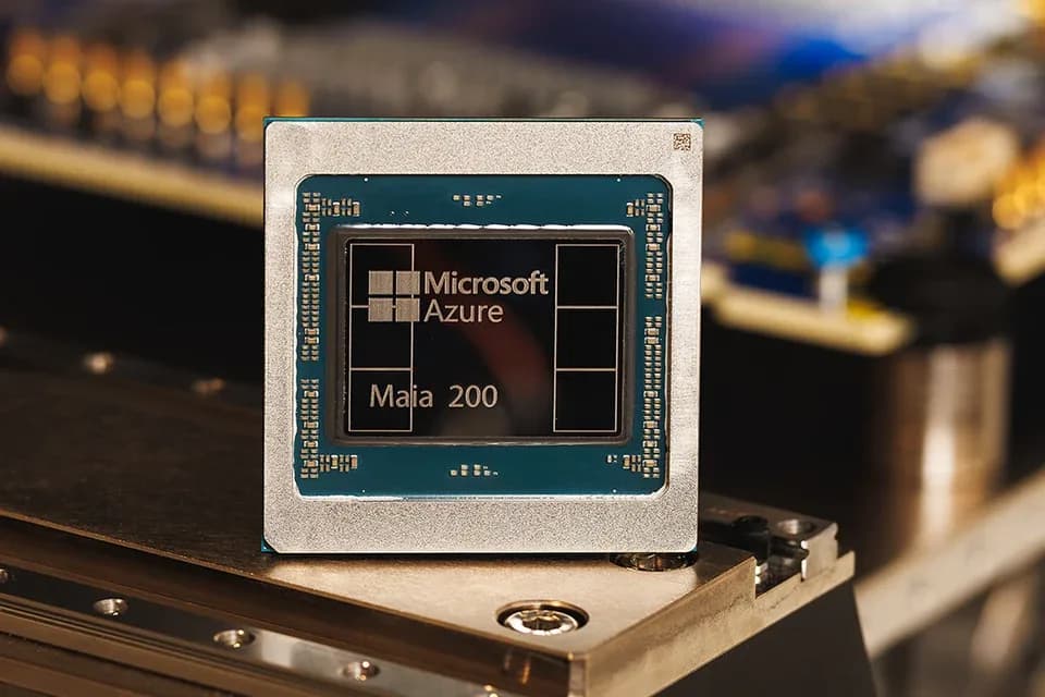
Microsoft's second-generation custom AI silicon packs over 140 billion transistors on TSMC N3 to deliver 10.1 PetaOPS of FP4 and over 5 PFLOPS of FP8 within a tight 750W TDP. Combining 216 GB of 7 TB/s HBM3e, 272 MB of software-managed SRAM, and an integrated Ethernet AI Transport Layer NIC, it scales cleanly to 6,144 accelerators.
Key Benchmarks & Specifications
Memory & BW216 GB HBM3e (7 TB/s) + 272 MB SRAMPeak Compute10.1 PetaOPS FP45+ PFLOPS FP8Scale-Up Fabric2.8 TB/s On-Die Ethernet ATL (6,144 Chips)Maker & Process Microsoft Azure (TSMC N3)TDP & System750W SoC TDPEditorial Strengths & Watchouts
+ Strengths / Pros
- +216 GB HBM3e (7 TB/s) plus 272 MB software-pinned CSRAM/TSRAM inside a 750W envelope
- +Integrated on-die 2.8 TB/s bidirectional NIC scales to 6,144 chips over standard Ethernet
- +10.1 PetaOPS native FP4 throughput engineered specifically for reasoning & agentic inference
− Watchouts / Trade-Offs
- −Restricted to Microsoft Azure regions with Maia SDK still in staged external rollout
- −Inference-first architecture rather than a merchant on-premise training chip
Eligibility & Access
- Best for Azure AI Foundry, Copilot, and enterprise inference workloads prioritizing FP4 tokens-per-dollar
Key Caveats to Verify
- Target narrow-precision FP8/FP4 quantization to unlock Maia 200's 2x–8x Tile Tensor Unit advantage
AWS's second-generation Annapurna Labs accelerator equips each Trn2 instance with 16 chips (1.5 TB HBM3, 46 TB/s bandwidth, 20.8 FP8 PFLOPS) and extends NeuronLink across 64 chips in Trn2 UltraServers for 83.2 PFLOPS of FP8 compute, 6 TB of shared HBM3, and 185 TB/s aggregate memory bandwidth.
Key Benchmarks & Specifications
Memory & BW96 GB HBM32.9 TB/s per Chip (6 TB UltraServer)Peak Compute1.3 PFLOPS FP8 (83.2 PFLOPS / 64-Chip UltraServer)Scale-Up Fabric NeuronLink (64 Chips) +12.8 Tbps EFAv3Maker & Process AWS Annapurna LabsTDP & System EC2 Trn2 (16×) & Trn2 UltraServer (64×)Editorial Strengths & Watchouts
+ Strengths / Pros
- +64-chip Trn2 UltraServers pool 6 TB of HBM3 and 185 TB/s bandwidth over NeuronLink
- +12.8 Tbps Nitro-encrypted EFAv3 scale-out networking scales to hundred-thousand-chip clusters
- +Substantial EC2 Capacity Block savings over comparable merchant GPU instances
− Watchouts / Trade-Offs
- −Requires compiling graphs and custom kernels through AWS Neuron SDK / NKI rather than CUDA
- −Per-chip 96 GB HBM3 trails 216–288 GB HBM3e chips until Trainium3 (144 GB) ramps
Eligibility & Access
- Best for AWS-native foundation model pre-training, Bedrock deployments, and high-volume batch inference
Key Caveats to Verify
- Profile torch.compile graphs with Neuron Explorer early to eliminate any eager-mode CPU fallbacks

Supercharging the proven Hopper architecture with 141 GB of HBM3e memory at 4.8 TB/s—1.8x the capacity and 1.4x the bandwidth of H100—the NVIDIA H200 delivers nearly 4 PFLOPS of FP8 compute in SXM baseboards and supports 4-way NVLink (564 GB pooled memory) in 600W air-cooled PCIe NVL servers.
Key Benchmarks & Specifications
Memory & BW141 GB HBM3e4.8 TB/sPeak Compute3,958 TFLOPS FP8 / INT8 (SXM)Scale-Up Fabric900 GB/s NVLink 4 (SXM)1.8 TB/s 4-Way NVLMaker & Process NVIDIA (TSMC4N Hopper)Editorial Strengths & Watchouts
+ Strengths / Pros
- +Direct Hopper compatibility with existing HGX H100 racks and air-cooled 600W PCIe servers
- +141 GB HBM3e holds 70B+ FP8 models comfortably on a single GPU with bigger KV-cache batches
- +Broadest global cloud and OEM server availability in 2026
− Watchouts / Trade-Offs
- −Lacks hardware FP4 Tensor Cores introduced on Blackwell B200 and AMD MI355X
- −Half the memory bandwidth (4.8 TB/s vs. 8.0 TB/s) of current-gen HBM3e flagships
Eligibility & Access
- Best for Enterprises expanding air-cooled on-premise AI clusters or needing immediate multi-cloud GPU capacity
Key Caveats to Verify
- Compare H200 NVL 4-way bridge topology against 8-way HGX SXM when sizing multi-GPU tensor parallelism

Eliminating inter-chip reticle boundaries altogether, Cerebras's 46,225 mm² Wafer-Scale Engine 3 integrates 4 trillion transistors, 900,000 AI cores, and 44 GB of on-wafer SRAM delivering 21 PB/s bandwidth (doubled to 43.2 PB/s and 250 PFLOPS on WSE-3 Turbo inside CS-4 racks).
Key Benchmarks & Specifications
Memory & BW44 GB On-Wafer SRAM21–43.2 PB/sPeak Compute125 PFLOPS (WSE-3)250 PFLOPS (WSE-3 Turbo)Scale-Up Fabric Single46,225 mm² Die (53.5 PB/s On-Wafer Fabric)Maker & Process Cerebras Systems (TSMC5nm Wafer)Editorial Strengths & Watchouts
+ Strengths / Pros
- +21–43.2 PB/s on-wafer SRAM bandwidth eliminates off-chip HBM bottlenecks during token decode
- +Disaggregated AWS Trainium prefill + Cerebras CS-3 decode architecture excels on agentic reasoning
- +Single-device programming model avoids complex 64-way GPU tensor-parallel debugging
− Watchouts / Trade-Offs
- −44 GB on-wafer SRAM requires multi-system clustering or weight streaming for frontier 400B+ models
- −Proprietary CS-3 / CS-4 appliance footprint rather than standard EIA server blades
Eligibility & Access
- Best for Ultra-fast interactive coding agents, deep test-time reasoning loops, and disaggregated cloud decode
Key Caveats to Verify
- Pair wafer-scale decode with high-HBM prefill clusters when serving massive long-context prompts

Designed compiler-first with zero hardware cache misses or dynamic packet arbitration, Groq's Language Processing Unit packs 230 MB of 80 TB/s SRAM on LPU v1 and scales to 500 MB of 150 TB/s SRAM per chip in 256-chip NVIDIA Groq 3 LPX racks built to run feed-forward decode alongside GPU attention.
Key Benchmarks & Specifications
Memory & BW230 MB–500 MB On-Chip SRAM80–150 TB/sPeak Compute Deterministic Compiler-Scheduled Tensor/VectorScale-Up Fabric Chip-to-Chip Plesiochronous /256-LPU LPX RackMaker & Process Groq / NVIDIA LPX Partner EcosystemTDP & System GroqNode Rack &256-Chip LPX Decode RackEditorial Strengths & Watchouts
+ Strengths / Pros
- +Deterministic compile-time execution guarantees sub-millisecond jitter-free time-per-output-token
- +80 TB/s (LPU v1) to 150 TB/s (Groq 3 LPX) internal SRAM bandwidth crushes low-batch decode latency
- +Ideal feed-forward specialist in disaggregated GPU-attention + LPU-decode racks
− Watchouts / Trade-Offs
- −230–500 MB SRAM per chip requires dozens to hundreds of LPUs to hold a single 70B+ model in memory
- −Strictly an inference engine with zero foundation-model training capability
Eligibility & Access
- Best for Real-time voice agents, speculative draft-token generation, and latency-critical interactive copilots
Key Caveats to Verify
- Evaluate total rack footprint carefully when serving high-concurrency long-context KV caches
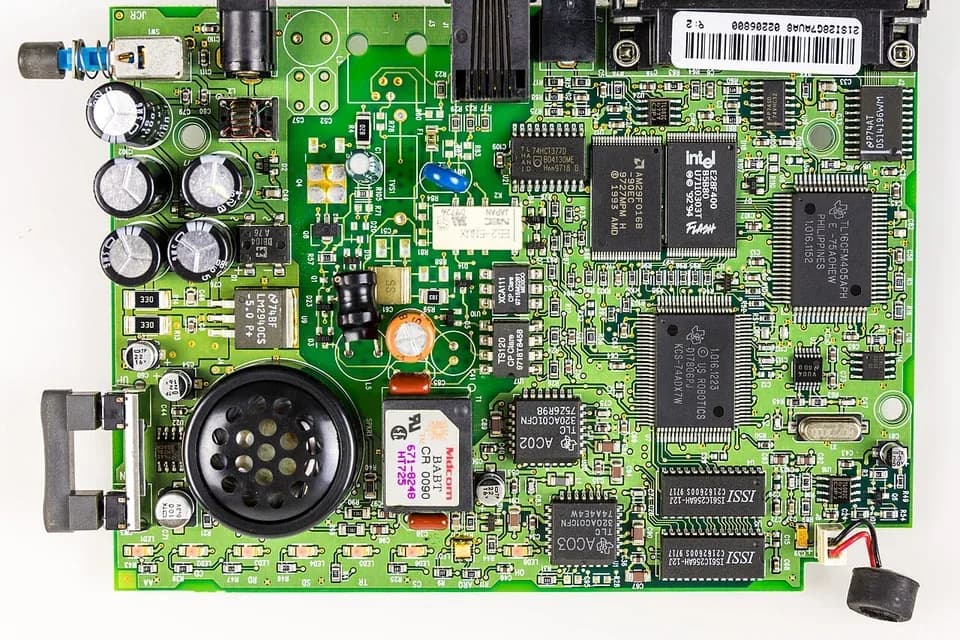
Built on TSMC 5nm with two compute dies bridged across an interposer, Intel Gaudi 3 combines eight large Matrix Multiplication Engines (1.8 PFLOPS FP8/BF16), 128 GB of HBM2e at 3.7 TB/s, and 24 integrated 200GbE RoCEv2 ports—available in both 8-way OAM baseboards and 600W HL-338 PCIe add-in cards.
Key Benchmarks & Specifications
Memory & BW128 GB HBM2e + 96 MB SRAM3.7 TB/sPeak Compute1.8 PFLOPS FP8 & BF16Scale-Up Fabric24× 200GbE Integrated RoCEv2 EthernetMaker & Process Intel / Habana Labs (TSMC5nm)TDP & System900W OAM MezzanineEditorial Strengths & Watchouts
+ Strengths / Pros
- +24 integrated 200GbE RoCEv2 ports eliminate proprietary fabric switches for scale-out clusters
- +128 GB HBM2e and 600W HL-338 PCIe cards fit standard enterprise Xeon servers cleanly
- +Native vLLM, PyTorch, and Hugging Face Optimum-Habana integration for open-weight LLMs
− Watchouts / Trade-Offs
- −HBM2e bandwidth (3.7 TB/s) and 1.8 PFLOPS FP8 trail HBM3e flagships like Blackwell and MI355X
- −Smaller third-party kernel developer community than CUDA or ROCm
Eligibility & Access
- Best for Cost-conscious enterprise RAG, fine-tuning, and open-Ethernet on-premise Dell or IBM Cloud deployments
Key Caveats to Verify
- Stick to well-supported Llama, Qwen, and Mistral vLLM paths for plug-and-play throughput
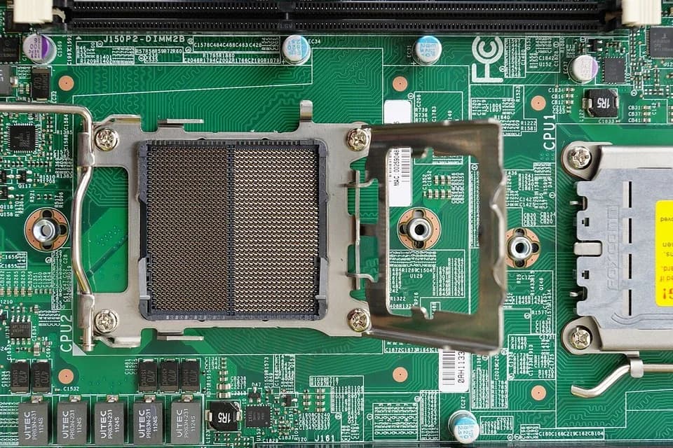
Co-designed for Meta's massive recommendation, ranking, and inference fleets across 16+ global regions, Next-Gen MTIA v2 packs an 8×8 processing-element grid on a 421 mm² TSMC 5nm die, delivering 708 sparse INT8 TFLOPS (354 dense), 256 MB of 2.7 TB/s on-chip SRAM, and 128 GB LPDDR5 at a frugal 90W TDP.
Key Benchmarks & Specifications
Memory & BW256 MB On-Chip SRAM (2.7 TB/s) + 128 GB LPDDR5Peak Compute708 TFLOPS INT8 (Sparse)354 TFLOPS BF16Scale-Up Fabric PCIe Gen5 Mesh + RDMA Scale-Out (72-Chip Rack)Maker & Process Meta Infrastructure (TSMC5nm)TDP & System90W TDPEditorial Strengths & Watchouts
+ Strengths / Pros
- +Ultra-efficient 90W TDP packs 72 accelerators into a single air-friendly rack
- +256 MB on-chip SRAM (2.7 TB/s) sustains high utilization even on low-batch real-time inference
- +Hardware-agnostic Triton-MTIA compiler integrates directly with PyTorch 2 TorchInductor
− Watchouts / Trade-Offs
- −Internal Meta datacenter silicon unavailable to external cloud customers
- −204.8 GB/s off-chip LPDDR5 targets DLRM ranking and medium inference rather than giant LLM pre-training
Eligibility & Access
- Best for Studying hyperscale GPU offloading, PyTorch 2 Triton custom ASIC compilation, and perf-per-watt co-design
Key Caveats to Verify
- Internal fleet accelerator—external teams should target AWS Trainium2, TPU v6e, or Azure Maia 200
Have a list idea?
Start your own list and get help drafting entries with AI. A free account is required.
Create a list with AI →Think something was robbed of a spot?
Nominate a missing contender — once approved, the community votes it up or down into the rankings.
Image credits
- NVIDIA Blackwell B200 & GB200 NVL72: en.wikipedia.org
- Google Cloud TPU v6e (Trillium): Visitor7 (CC BY-SA 3.0)
- AMD Instinct MI355X: Festival Internacional de Cine en Guadalajara (CC BY 2.0)
- Microsoft Azure Maia 200: Microsoft Azure (TSMC N3) Official Hardware Press Release
- AWS Trainium2 (EC2 Trn2 UltraServer): beebom.com
- NVIDIA H200 Tensor Core GPU: garageaquatics.com
- Cerebras Wafer-Scale Engine 3 (WSE-3 / WSE-3T): sipthestyle.com
- Groq LPU & NVIDIA Groq 3 LPX: blog.panterranetworks.com
- Intel Gaudi 3 AI Accelerator: Raimond Spekking (CC BY-SA 4.0)
- Meta Next-Gen MTIA v2: smial (talk) (FAL)
Rank it your way
Remix this list into your own ranking, or head to the play hub for every game mode and community breakdown — blind mode, challenges, tier lists, and more.